
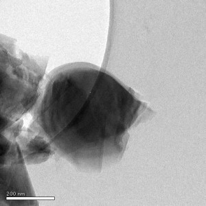
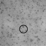
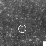
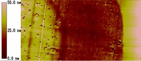
Z-Constrast with High Angle Annular Dark-Field STEM
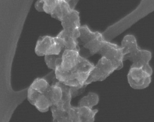
Scanning transmission electron microscopy (STEM) images of a Zn-containing polymer, acquired on the JEOL 2010F STEM (recently retired from the facility in 2018). The images show numerous Zn-rich domains approximately 2.5 nm in diameter. These aggregates enhance the physical properties of the material.
The image in (a) was acquired in bright field STEM, in which the electron density difference between Zn-rich domains and the matrix polymer serves as the contrast mechanism. The aggregates appear dark, without the need for chemical staining which may alter the size of the features.
The image in (b) was acquired in high-angle annular dark field STEM, in which the high atomic number of the Zn-rich domains serves as the contrast mechanism. The aggregates appear bright, confirming that they contain high-atomic-number Zn atoms. Complete correspondence of the features in (a) and (b) is indicated by the circles.
Laurer, J.H.; Winey, K.I. Macromolecules 31(25), 9106-9108, 1998.
Energy Filtered TEM
These images were collected using the Gatan Image Filter on the JEOL 2010F TEM/STEM from a BN sample dispersed on a holey carbon film. The electron energy loss spectrum shows families of peaks for B, C, and N in order of increasing energy loss (upper left). The images at the upper right and lower left are EFTEM maps for B and C, respectively. The image on the lower right represents a combined map for B (blue) and C (yellow).
Energy Filtered TEM Spectrum Image
In addition to EFTEM imaging, the Gatan Image Filter on the JEOL 2010F TEM/STEM (recently retired from the facility 2018) can be configured to collect a series of image slices through the electron energy loss spectrum. The upper images show a spectrum and TEM image of BN grains on a carbon film. The lower image shows an animated view of the energy slices collected from 150 eV to 420 eV in 10 eV increments. As the animation runs, the BN grains get brighter at ~180 eV and ~400 eV as the energy slices intersect the B and N edges, respectively. At an energy of ~280 eV, the carbon film gets brighter due to the C edge in the EELS spectrum.
X-ray Mapping of a Paint Chip
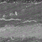
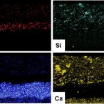
These images were collected using the JEOL 6300F HRSEM and the PGT IMIX EDS workstation. The sample is a paint chip that was sectioned normal to the successive layers of paint. The maps clearly show the compositional heterogeneity of the sample. The results of the study revealed the transition from lead-based paint to a paint rich in titanium, calcium and silicon.
Dark-Field STEM Imaging of Pd Nanoparticles on a Zeolite
High-angle annular Dark field imaging in STEM mode on the JEOL 2010F TEM/STEM (recently retired from the facility 2018) is one of the most powerful techniques for the characterization of metalic nanoparticles on catalyst particles. The Pd particles in this image range from 2 to 10 nm.
Low kV SEM Imaging of Collagen
This image was collected with our 6300FV SEM at 1 kV from an uncoated sample of collagen. Scanning Electron Microscopes, like the 6300FV, which are mounted with a field emission gun dramatically increase the productivity of our facility by allowing for the low kV imaging of uncoated, beam sensitive samples.
SEM Imaging of a Neuron Bundle
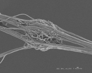
This is an SEM image of a bundle of neurons grown from culture taken on the JEOL 6300F HRSEM. The bundle is suspended between two protein coated surfaces.
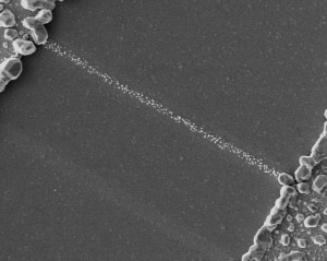
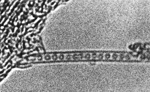
Growth of Pd Between Zeolite Particles
This image, collected on the JEOL 2010F TEM/STEM in dark field STEM mode, appears to be a bridge of Pd that has formed between adjacent zeolite particles.
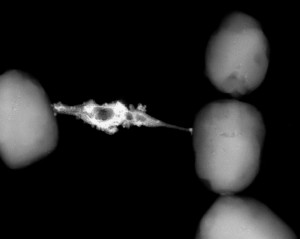
Low kV SEM Imaging of Cells on Polymer Spheres
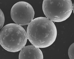
This image was collected with our 6300FV SEM at 1 kV from an uncoated sample of cells that had been grown on polymer spheres.
SEM Imaging of Oriented Polymer Fibers
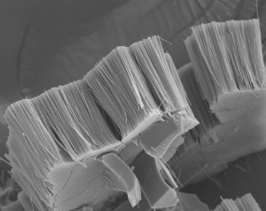
This image was collected with our 6300FV SEM at 1 kV from a carbon coated sample of oriented polymer fibers.
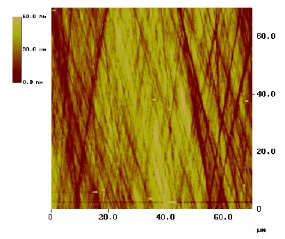
Atomic Force Microscopy
Circuit fabrication using AFM manipulation.
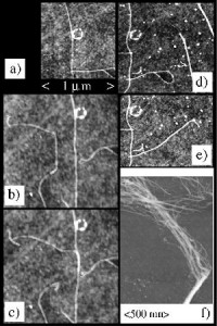
The experiment begins with one vertical tube (main tube) and one horizontal tube (lasso tube) (a). A tube is then brought in close proximity to the main tube (b) and the tube is pushed against (perhaps on top of) the main tube (c). Additional tubes are then manipulated on top of the main tube (d). Finally, the lasso tube is opened and unwanted tubes are pushed away (e). Image (f) shows some unraveling of the nanotubes that has occurred as a result of the AFM manipulation.
J. Lefebvre, J. F. Lynch, M. Llaguno, M. Radosavljevic and A. T. Johnson, Single-wall carbon nanotube circuits assembled with an atomic force microscope, Appl. Phys. Lett. 75, 3014-3016(1999).
Nanofabrication & Nanodevices
Nanoparticle Wire
This sample consists of a thin film of PZT with microfabricated gold electrodes. Between the two gold electrodes a line has been patterned using a combination of AFM lithography followed by photodeposition. The line is made up of silver nanoparticles. Average particle size is 50nm.
Structural Studies
Another nanotube surprise: Buckypeas in a pod
One of the latest additions to the expanding menagerie of carbon nanostructures is the single walled carbon nanotube (SWNT) that encapsulates a string of spherical C60 molecules. Each C60 is only 0.7 nm in diameter and appears as a circle in the high resolution micrograph shown above.
This nanoscopic peapod was announced by its discoverers, Brian Smith (Penn), David Luzzi (Penn) and Marc Monthioux (CEMES, France), in Nature [396, 323 (1998)]. Utilizing the high resolution imaging and in-situ capabilities of the TEMs in the facility, the encapsulated buckyballs are seen to move back and forth inside the nanotubes, lining up in groups of two, three, or more — just like arrangements of beads on an abacus.
This finding opens a new field in nanotube research and could conceivably affect the interpretation of earlier results, which were obtained with the supposition that the tubes are empty. “Very, very cool — just mind-blowing” commented fullerene researcher Daniel Colbert (Rice). “I think they probably will end up teaching us something about the nucleation and growth of nanotubes.”
excerpted in part from Chemical & Engineering News 77 (2), 32 (1999)
High Resolution Image of a Zeolite
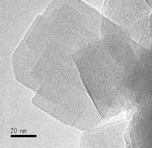
High resolution image of a zeolite collected on the JEOL 2010F STEM/STEM (recently retired from the facility 2018).
Imaging of La2C60 molecules inside of a Nanotube
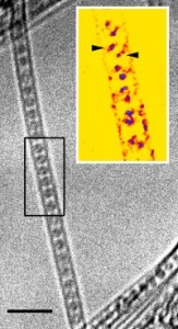
TEM micrograph (JEOL 2010F – recently retired froo the facility 2018) of a carbon nanotube containing molecules of La2C80. The color inset emphasizes the ability to image the two individual La atoms in each molecule (also seen in the main figure as darker features).
AFM Imaging of Carbon Nanotubes
This is a tapping mode AFM image of a bundle of carbon nanotubes collected using the Digital Instruments Multimode AFM. Courtesy of Marko Radosavljevic, Dept. of Physics, University of Pennsylvania.
MFM Image of a Computer Harddisk
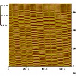
Topography of 750MB disk acquired in Tapping Mode(left). Frequency contrast image acquired in Interleave Mode (right). We were able to calculate the storage capacity of this disk from the MFM image. Please note that MFM image is unaffected by topography. Courtesy of Tony Alvarez
Scanning Surface Potential Image of SrTiO3
SSPM image of charge redistributed on an SrTiO3 surface using EFM. Courtesy Sergei Kalinin.
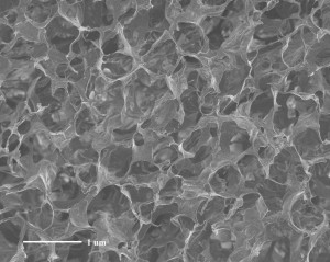
Scanning Surface Potential Image of ZnO
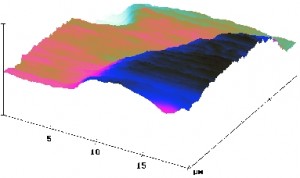
Phase Imaging of a Coated Fiber

Topography (left) and Phase Image (right) of a coated fiber. Note that the phase image demonstrates the presence of the diffusion of a foreign material. This foreign material does not show up in topography. Courtesy Tony Alvarez and Anthony Ribaudo of Honeywell.
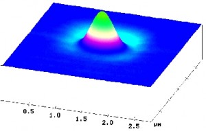
Tapping Mode AFM Image Using a Fluid Cell
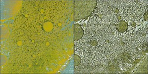
Fluid tapping mode AFM allows real time three dimensional imaging of biological systems in liquid environments. This 10um x 10um area shows domains in a Langmuir Blogett (LB) film. The smallest domain size is ~40nm. This image was collected under a physiological buffer solution using the Dimension 3000 in Fluid Tapping mode AFM. The right image is the surface topography and the left image is the simultaneous phase contrast image.
Electrical Property Measurement using AFM
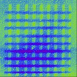
This is an example of AFM imaging differences in electrical properties in a material. A patterned surface of a conductive polymer was imaged using two different SPM modes (image dimension 40mm x 40mm). Before imaging, on and off states were written using the AFM. The right image is a SSPM image showing localization of charge. Dark areas are more negative than light areas. The left image is a SCM image showing the corresponding change in conductivity of the film. Green areas are more metallic than blue.
Surface Studies – Ion Beam Analysis
Rutherford Backscattered Spectra of a PZT Film
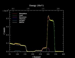
This a Rutherford backscattered spectra collected from a 4600A PZT film deposited on a Si substrate. The simulated film composition is Pb(Zr0.52Ti0.48)O3. The data were collected at normal incidence with a 2.0 MeV He+ beam.
Surface Studies – Ion Beam Analysis
Rutherford Backscattered Spectra of a CeO Film
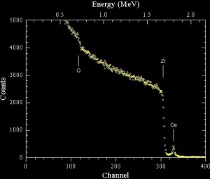
This a Rutherford backscattered spectra collected from a 20A CeO film deposited on a ZrO substrate. The data was collected at normal incidence with a 2.0 MeV He+ beam.
PMMA-Grafted Gold Nanoparticles in a
Polymer Blend Matrix (PMMA:SAN)
Here, 0.5vol% of PMMA-grafted gold nanoparticles* are dispersed into a solution of PMMA:SAN (50:50) in MIBK, followed by spin-coating to make homogeneous composite film with a thickness of ~120nm. Fig (a) shows homogeneous depth distribution of gold particles with some substrate segregation, due to the preannealing process used to remove the solvent (120°C, 24hr). After annealing at high temperature (200°C, 5hr), preferential wetting of PMMA at the surface and substrate caused redistribution of gold particles along with the PMMA phase, leading to a pseudo-trilayer formation in Fig (b). Glancing angle technique (75° tilt of sample goniometer) was used to improve depth resolution.
Submitted by Hyun-joong Chung, Department of Materials Science and Engineering
* PMMA-grafted gold nanoparticles (~2.7nm, MPMMA=27[Kda]) were kindly provided by Dr. Kohji Ohno in Kyoto University.
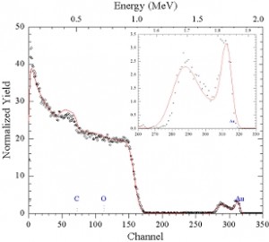
Segregation of Nanoparticles to the Surface of an Annealed Polymer
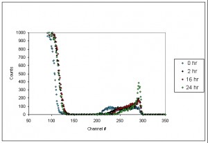
Rutherford backscattered spectroscopy was conducted on a polymer blend sample containing metal nanoparticles. The polymer/nanoparticle mixture was deposited as a 600 nm thick film on a silicon wafer by spin casting. With increased annealing at 185oC, the metal nanoparticles undergo diffusion towards the polymer surface as is indicated by the movement of the metal peaks (channel numbers 200 – 300) to higher channel number (higher energy).
Submitted by Ranjan Deshmukh, Department of Materials Science and Engineering.


